Back to Course
Microelectronics Materials and Devices
0% Complete
0/0 Steps
-
Introduction3 Topics
-
Crystal Structure17 Topics
-
Semiconductor Devices in Microelectronics
-
Atom Arrangement (Carbon) vs Material Property
-
Crystal Structure and Ordering
-
Crystal Structure
-
Cubic Lattices
-
Derivatives of FCC Lattices
-
Hexagonal Lattices
-
Cubic Close Packing
-
Hexagonal Close Packing
-
Atomic Packing Factor
-
Planes and Directions
-
Directions in Crystal
-
Applications of Miller Indices: Si Wafers
-
Crystallographic Orientation
-
Crystal Plane and Crystal Direction
-
Experimental Determination of Crystal Structure & Properties
-
Summary and Learning Outcomes
-
Semiconductor Devices in Microelectronics
-
Energy Bands
-
Dielectrics and Other Non-semiconductor Materials
-
Semiconductors
-
P-N Junctions
-
MOS Capacitors
-
Metal Semiconductor Contacts
Lesson Progress
0% Complete

Renewable Energy – solar cells

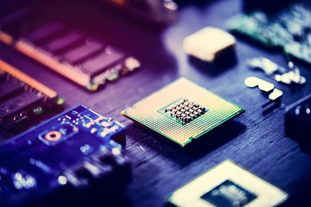
Internet of Things – processors

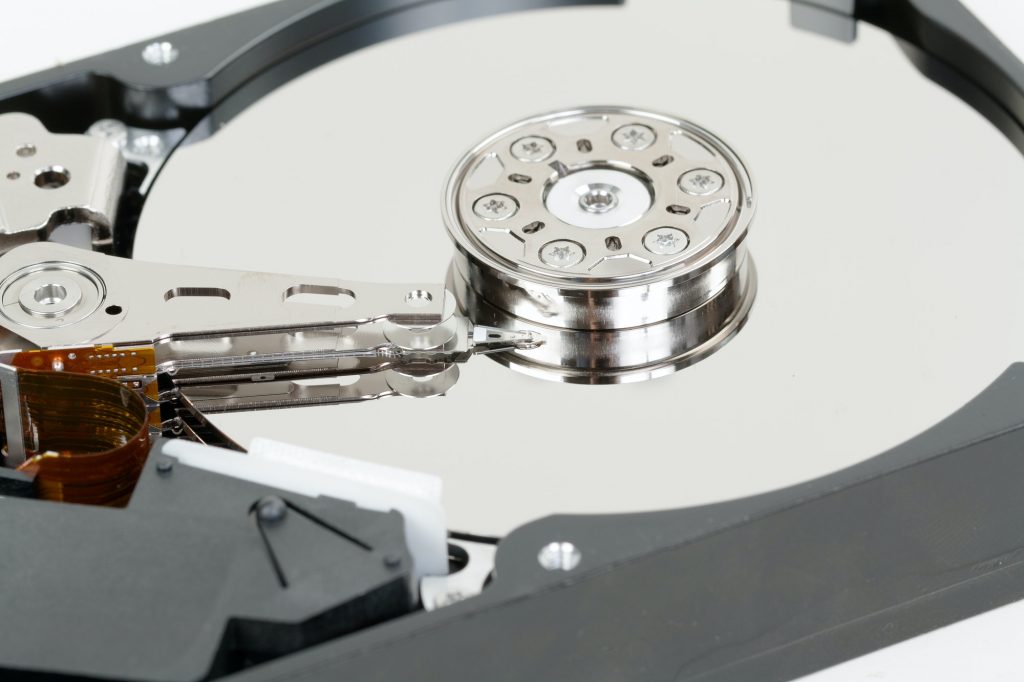
Information Storage – memory

Robotics and Automation—sensors and MEMS devices


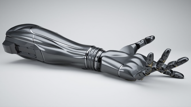
Medical devices —sensors, lab-on-chip
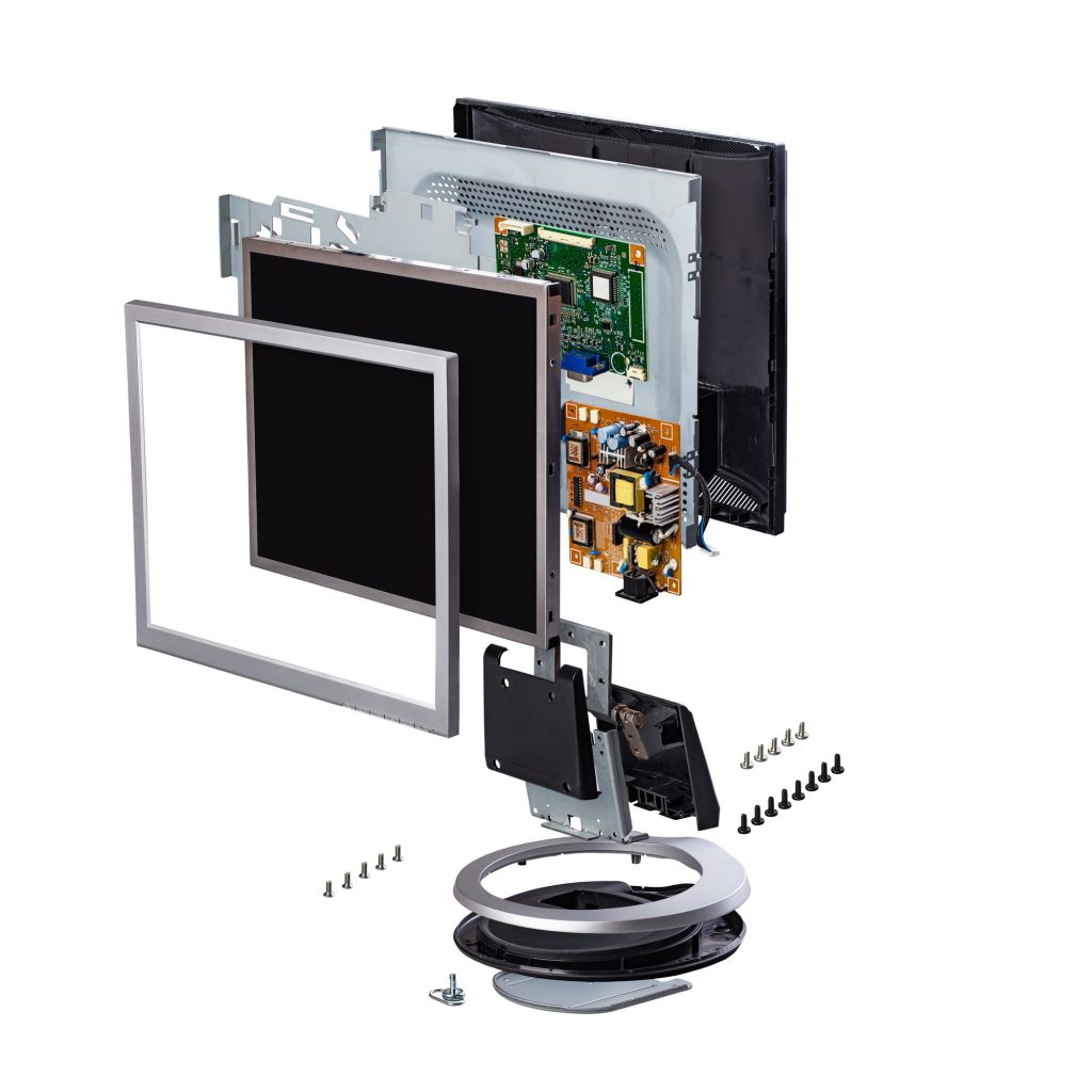
Displays—LED, LCD

Personal electronics – displays, sensors

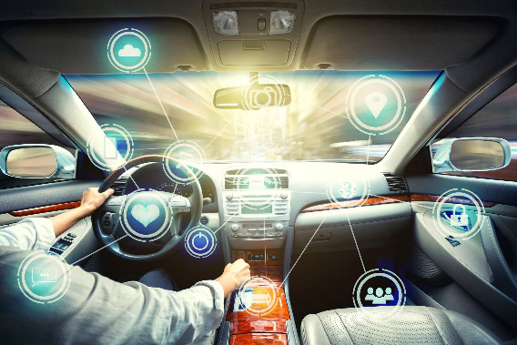
Transportation- nanomaterials, intelligent sensors

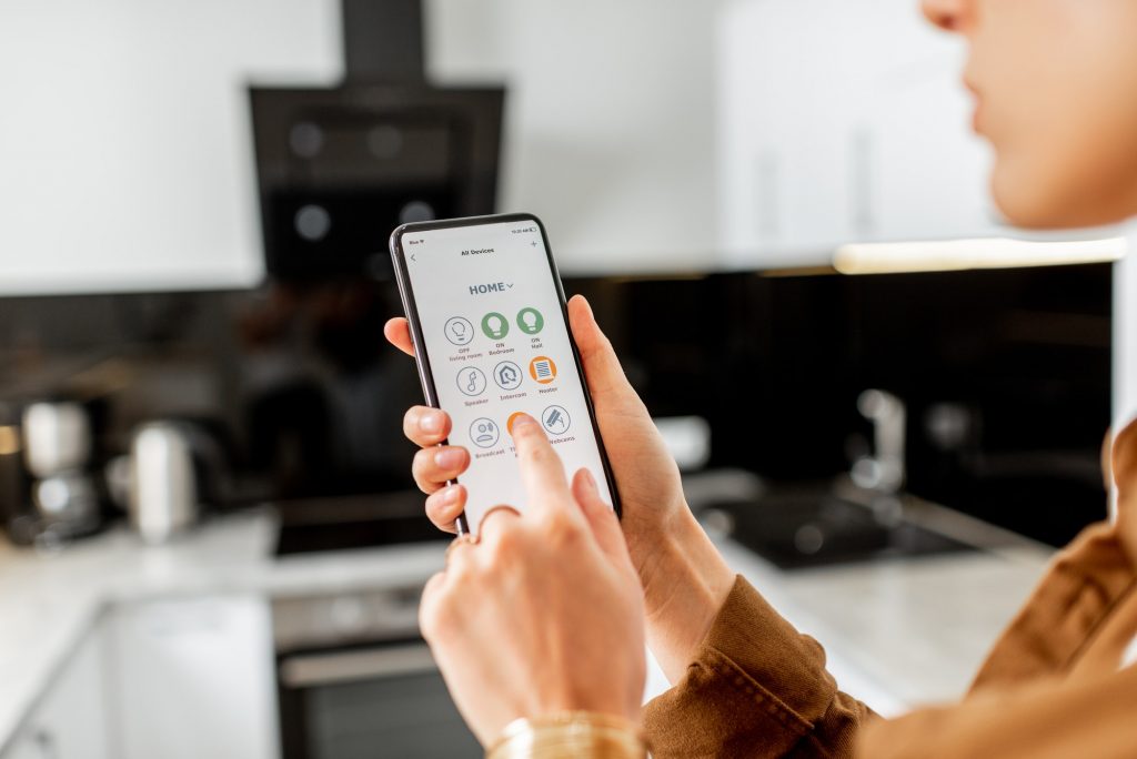
Portable Electronics – sensors, processors, smart materials/screens

Flexible electronics–nanomaterials
